Using a VNA to design antennas for GPS interference detection
This article appeared in Microwaves and RF and has been published here with permission.
Introduction
GPS interference can come in many forms. The most well-known is intentional jamming or spoofing, denying GPS for (typically nefarious) reasons – it is common knowledge that parts of the Middle East are denied GPS service, and there have been cases of ships in the Black Sea suddenly reporting being located 25 nautical miles away, inland, at an airport.
There are also a number of recorded cases of unintentional interference from a variety of sources. Real-life examples that come to mind include a worn cable in a car shark-fin antenna causing the entire roof to radiate; a waterlogged antenna on a building re-radiating and jamming nearby GPS antennas; and even the output of a GNSS simulator accidentally left unterminated after an exhibition demonstration! Being able to quickly determine the presence of GPS interference, and its direction of arrival, is vital in both civilian and defense applications.
GPS signals are very weak – below the thermal noise floor. A GPS receiver needs to boost the SNR (Signal-to-Noise Ratio) to acceptable levels using process gain; That is, by knowing in advance the precise sequence it is looking for, a receiver can distinguish the signal from the noise. The process gain is sufficient to identify a signal in a typical environment's noise level. However, if the noise level is higher than normal then the process gain can be insufficient, at which point the receiver is jammed. Fortunately, the GPS L1 frequency (a 20 MHz band centered on 1575.42 MHz) is a protected frequency and radiation in this band is tightly controlled.
How to detect GPS interference
A typical GPS jammer works by increasing the interference, or noise, in the specific band of interest. The signal does not need to contain any information; it just needs to drown out the already quiet GPS signal. Unintentional radiators also jam in this way. A single tone at the right frequency could jam GPS, but many jammers use a frequency sweep over a small band to relax manufacturing tolerance requirements. Because the GPS L1 frequency is protected and the GPS signal is below the noise floor, any detectable signal in the band of interest must be interference.
Spoofing is a much more complicated subject, but evidence shows that the signal needs to be strong enough to overcome the true GPS signal and so is likely to still be detectable using a received signal strength (RSSI)-based method.
To make a GPS interference detector, then, a receiver need not be any more complicated than an antenna and a power detector. A logarithmic amplifier, which returns a voltage proportional to the received power, plus an ADC, would suffice. The system should have a narrow bandwidth centered on the L1 band to avoid false positives. To detect just the presence of jamming (and not its source) then the receive antenna should have a wide beamwidth.
Rather than adding more components to create a bandpass filter, with care an antenna can function as a basic filter. This is easier when targeting a single narrow frequency such as the GPS band, rather than trying to capture a wide band or multiple bands.
A patch antenna is easy to fabricate: the simplest form is an area of copper on a piece of FR4 PCB material, and can be made at any PCB manufacturer or even on a prototyping router.
A basic patch antenna meets both requirements of being narrow bandwidth and wide beamwidth. Basic patch antennas are typically fairly narrowband and single patch has a roughly hemispheric beam pattern.
The intricacies of designing a patch antenna are beyond the scope of this article. Simulation software ensures that a designer can have a good amount of confidence in their design without having to spend time waiting for hardware. However, a simulation can only take into account what is known and measured – reality will always come with unmodelled factors and hardware test is an inevitable step in design. A VNA is the ideal piece of equipment for validating an antenna design.
Validating the patch antenna
Testing an antenna with a VNA will result in the antenna radiating. GPS L1 is a protected frequency, meaning broadcase in the band is tightly controlled. Normally, when testing a passive device such as an antenna, the VNA would be set to its maximum power output to achieve the best SNR. A PicoVNA has a maximum output power of 10 dBm, or 0.01 W. The EU harmonized standard for (industrial) EMC specifies a maximum emission level of 70 dB(µV/m), equivalent to 3.2 mV/m, at 3 m from the emitter. A 10 dBm signal into an antenna with a radiation efficiency of 0.5 would generate a 129 mV/m field, over 40 times the limit. This assumes an isotropic antenna – including antenna directivity, the field strength would be even higher. To remain under the limit, the input power would have to be at most -74 dBm.
It is important to understand what different measurements can be made on a VNA and what information they can and cannot give.
The overall gain of an antenna (not including the radiation pattern) is determined by two, somewhat independent, factors. The first is the match between the antenna and its feed network – the antenna input match. The quality of this match determines how much of the signal source's energy is successfully transmitted into the antenna. The second is the match between the antenna (perhaps its "output" impedance) and free space: the antenna radiation efficiency, which indicates how much of the RF energy successfully delivered to the antenna is radiated into free space. Both parameters combine to create the antenna gain.
Measuring the S11 of an antenna only quantifies the input match and not the radiation efficiency, and therefore not the antenna gain as a whole, but it is much simpler to conduct than a two-port S21 measurement.
Consider a generic S11 measurement of a black box device under test (DUT); neglect that the DUT is an antenna. When measuring S11 the smallest amount of reflection occurs when the input impedance of the DUT best matches the VNA. With a good match the majority of the signal is successfully transmitted into the DUT. Mismatches increase the proportion of power reflected.
A mismatch could be at the DUT, but it could also be from the VNA. The purpose of a VNA calibration is to correct for any inherent errors in the VNA and test fixtures (the cables and connectors used between the VNA and the DUT). One source of VNA port mismatch is the port directivity. "Directivity" is a somewhat misleading term for an antenna engineer, but it refers to the directional coupler at the output of the VNA port; any non-ideal VNA port directivity is due to the leakage between two of the directional coupler's ports. The calibration process measures, among other things, the leakage between the directional coupler's ports, allowing a calibrated VNA to correct for it in measurements.
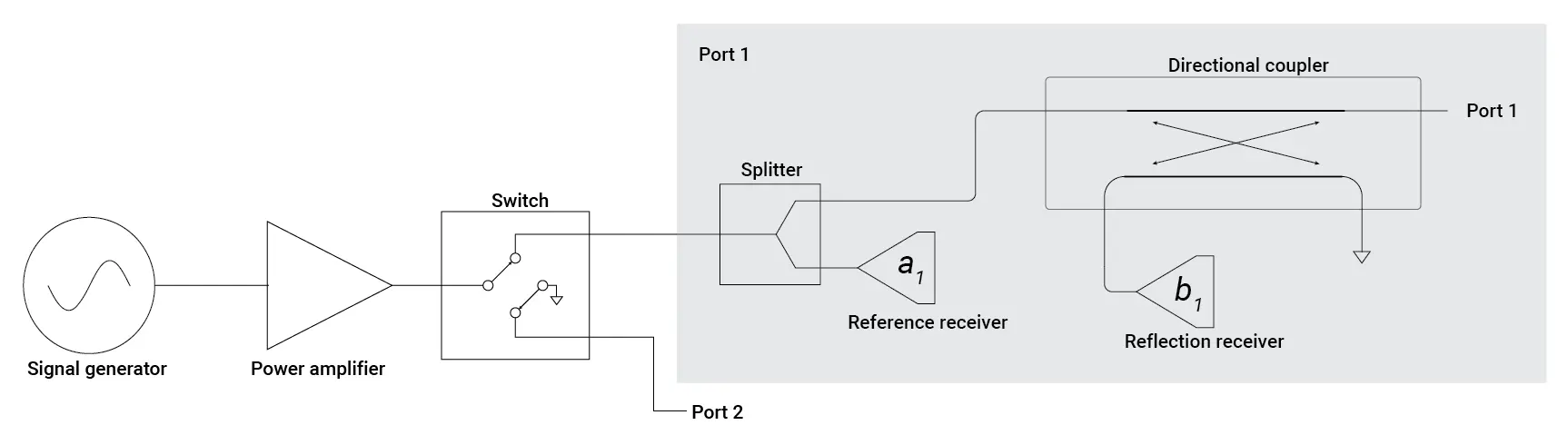
Most VNAs have a four-receiver architecture (Fig. 1). In this design, the VNA generates the source signal. After the signal generator, the signal is split: one portion is for the reference receiver, a1, which measures the signal level before it leaves the port. The other portion goes to the port via the directional coupler. The DUT is connected to the through port of the directional coupler. Signal that is reflected back couples across and is measured by the reflection receiver, b1.
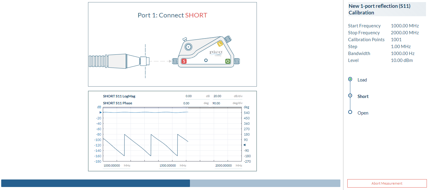
During calibration, the VNA generates a frequency sweep. It then measures the signal at a1 and at b1. A known DUT (the calibration standard) means the VNA can calculate from these measurements the leakage through the directional coupler with frequency. Applying the calibration then corrects for the leakage. Any imperfection in the calibration, or rounding errors in calculation, will affect this correction and therefore the effective directivity after calibration. Any error in the effective directivity can add to or subtract from the measured return loss of the DUT and the exact effect will vary with frequency.
Regarding calibration kits, there are two main approaches. The first approach has the various parts of the kit (load, short, open) precisely match a pre-defined set of polynomial coefficients. The second has the kit measured after manufacture, preferably with measurements traceable back to national standards. The precise measurements, in the form of a look-up table unique to a calibration kit serial number, are then used by the VNA during the calibration process. Both approaches can deliver the same level of accuracy.
When carrying out high precision measurements it is important to have traceable standards; the calibration is only as good as the calibration kit. The kit's parameters will have been measured by another piece of equipment, which will have its own errors. And that piece of equipment will have been measured by another, with its own errors... A good quality calibration kit will have every error in its characterization process quantified and traced back to national standards. The directivity, for example, is affected by the load match. It is crucial to know the exact impedance across the frequency sweep to achieve a good calibration.
Errors during calibration have a number of potential sources. The most common are related to incorrectly tightening cables and connectors. Lower quality cables have lower phase and gain stability and so if the cables are moved between calibration and test then the characteristics could change. Calibrations can be checked during the process if a graph is displayed (such as in Fig. 2), or by using a check standard after calibration.
Regarding antennas, then: The input efficiency of the antenna depends on the match between the feed (the VNA in this measurement) and the antenna input. The radiation efficiency is therefore determined by how well the antenna matches free space. As these are two separate ports, the frequency with the lowest S11 may not be the antenna's resonant frequency. The impedance of an antenna also varies hugely with frequency – this is what determines the bandwidth of an antenna.
If the input impedance of an antenna does not determine all of the antenna gain, and the input impedance of the antenna changes with frequency, and changes in impedance affect the directivity of a VNA, it is clear to see how measuring the S11 of an antenna alone could give misleading results.
Further measurements
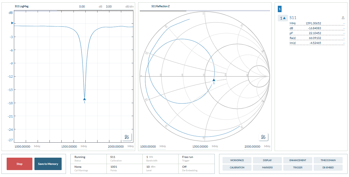
The best S11 result would be when the antenna input impedance best matches the VNA port impedance, but in a final design the VNA will not be the signal source nor receiver. The antenna design must be matched to the feed network. A VNA can measure the real and imaginary components of the input and aid with matching, as shown in Fig. 3.
An S21 measurement is the gold standard for characterizing an antenna, with port 1 connected to the antenna under test and a second antenna – well characterized, with a known frequency response – on port 2. An S21 measurement will determine the total antenna gain with frequency, and can also be used to measure the beam pattern.
To gain an accurate picture, sufficient signal strength for the received signal to be within the dynamic range of the VNA. This is unlikely to be possible while staying within the radiated emissions limits and therefore a proper test site is a must.
Detecting jamming
With a narrowband patch antenna tuned to GPS L1, the receiver needs only be an amplifier and a power detector. Designing a basic GPS jamming detection system is a simple task, assuming appropriate care is taken to get accurate measurements. With this simple hardware (an antenna plus a power detector) it is quick to confirm the presence of jamming, saving time diagnosing equipment malfunctions.
References:
Handbook of Microwave Component Measurements with Advanced VNA Techniques, Joel P Dunsmore, 2nd ed.
EN 55011:2016 + A11:2020 Industrial, scientific and medical equipment. Radio-frequency disturbance characteristics. Limits and methods of measurement